- 您现在的位置:买卖IC网 > Sheet目录527 > SX1210I084T (Semtech)IC SINGLE-CHIP RECEIVER 32-TQFN
SX1210
ADVANCED COMMUNICATIONS & SENSING
5. Data Processing
5.1. Overview
5.1.1. Block Diagram
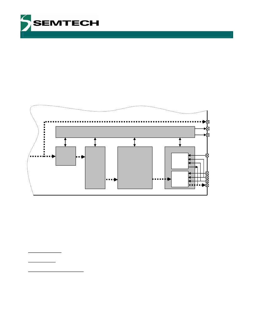
Figure 19, illustrates the SX1210 data processing circuit. Its role is to interface the data from the demodulator and
the uC access points (SPI, IRQ and DATA pins). It also controls all the configuration registers.
The circuit contains several control blocks which are described in the following paragraphs.
Rx
SX1210
DATA
CONTROL
IRQ_0
IRQ_1
Data
Rx
SYNC
SPI
Tx
RECOG.
PACKET
HANDLER
FIFO
(+SR)
CONFIG
DATA
NSS_DATA
SCK
MOSI
MISO
Figure 19: SX1210’s Data Processing Conceptual View
The SX1210 implements several data operation modes, each with their own data path through the data processing
section. Depending on the data operation mode selected, some control blocks are active whilst others remain
disabled.
5.1.2. Data Operation Modes
The SX1210 has three different data operation modes selectable by the user:
Continuous mode : each bit received is accessed in real time at the DATA pin. This mode may be used if
adequate external signal processing is available.
Buffered mode : each byte received is stored in a FIFO and accessed via the SPI bus. uC processing overhead
is hence significantly reduced compared to Continuous mode operation. The packet length is unlimited.
Packet mode (recommended) : user only retrieves payload bytes to/from the FIFO. Sync word is automatically
detected and stripped off while optional CRC check and DC free data decoding can be performed. The uC
processing overhead is hence reduced further compared to Buffered mode. The maximum payload length is
limited to the maximum FIFO limit of 64 bytes
Rev 2– Sept 8 , 2008
th
Page 28 of 73
www.semtech.com
发布紧急采购,3分钟左右您将得到回复。
相关PDF资料
SX1211SK915
KIT STARTER FOR SX1211 915MHZ
SX1211SKA915
KIT STARTER FOR SX1211 915MHZ
SX1223SK868
KIT STARTER FOR XE1223 868MHZ
SX1231-31SKB915
TVS
SX1240SKA433
TVS
SX1701BI085TRT
IC AMP 2.5GHZ 5.3V 16-MLPQ
TA002-10002
LED HEATSINK W/FAN 12V 40X10MM
TC620HEPA
IC TEMP SNSR 5V DUAL TRIP 8-DIP
相关代理商/技术参数
SX1210I084TRT
制造商:Semtech Corporation 功能描述: 制造商:Semtech Corporation 功能描述:IC SINGLE-CHIP RECEIVER 32-TQFN 制造商:Semtech Corporation 功能描述:SX1210 Series 863 to 960 MHz 3 V 200 kbps Ultra Low Power Receiver - TQFN-32
SX1211
制造商:SEMTECH 制造商全称:Semtech Corporation 功能描述:Lowest Power Integrated UHF Transceiver Short Range Devices
SX1211_08
制造商:SEMTECH 制造商全称:Semtech Corporation 功能描述:Ultra-Low Power Integrated UHF Transceiver
SX1211-11SKA868
功能描述:KIT STARTER FOR SX1211 868MHZ RoHS:是 类别:RF/IF 和 RFID >> RF 评估和开发套件,板 系列:- 标准包装:1 系列:- 类型:GPS 接收器 频率:1575MHz 适用于相关产品:- 已供物品:模块 其它名称:SER3796
SX1211-11SKA915
功能描述:KIT USB FOR SX1211 TXRX 915MHZ RoHS:是 类别:RF/IF 和 RFID >> RF 评估和开发套件,板 系列:- 标准包装:1 系列:- 类型:GPS 接收器 频率:1575MHz 适用于相关产品:- 已供物品:模块 其它名称:SER3796
SX1211I084T
制造商:Semtech Corporation 功能描述:
SX1211I084TRT
功能描述:IC SNGL-CHIP TXRX 32-TQFN RoHS:是 类别:RF/IF 和 RFID >> RF 收发器 系列:- 产品培训模块:Lead (SnPb) Finish for COTS
Obsolescence Mitigation Program 标准包装:30 系列:- 频率:4.9GHz ~ 5.9GHz 数据传输率 - 最大:54Mbps 调制或协议:* 应用:* 功率 - 输出:-3dBm 灵敏度:- 电源电压:2.7 V ~ 3.6 V 电流 - 接收:* 电流 - 传输:* 数据接口:PCB,表面贴装 存储容量:- 天线连接器:PCB,表面贴装 工作温度:-25°C ~ 85°C 封装/外壳:68-TQFN 裸露焊盘 包装:管件
SX1211I084TRT
制造商:Semtech Corporation 功能描述:GPSS WL SKU APP1
